Imagine a material that’s so thin it’s essentially two-dimensional. Now, imagine it’s able to form spontaneously on different surfaces and change the properties of these surfaces in multiple ways. It’s one of the wonders brought to us by nanoscience, and this type of structure is called a “self-assembling monolayer”.
This type of technology is now widely used in a number of applications, from medicine and electronics to sensing. Four researchers who pioneered various aspects of self-assembling monolayers were recently awarded the prestigious Kavli prize to celebrate their achievements in the field: David L. Allara (USA), Ralph G. Nuzzo (USA), Jacob Sagiv (Israel), and George Whitesides (USA).
We take a lot of materials we use today for granted, but many of them were developed relatively recently — and their existence makes the technology around us possible. Some of this innovation happens at the very surface of materials, which is where we interact with them.
The concept of self-assembled monolayers has been floating around for about a century, but for a long time, this was only restricted to liquid films. The first films were invented by Katharine Blodgett and Irving Langmuir, but these only formed at the interface between air and liquid.
The field of deploying monolayers on solid surfaces starts with the work of Jacob Sagiv. In a landmark paper from 1980, Sagiv showed that some molecules could be bound on the surfaces of some materials, which he suggested could be used in a number of applications. He was right: if we fast forward to the 2010-2020 decade, there are some 400-500 patents filed every year for this type of technology.

Just three years later, Ralph Nuzzo and David Allara, working at the now-legendary Bell Labs, achieved another milestone: they showed that films of molecules can be adsorbed onto glass and metal surfaces (adsorbtion being adhesion of atoms, ions or molecules to a surface. This is important for a number of reasons; first of all, it expanded the range of usable surfaces and layer molecules. But Nuzzo and Allara also accurately estimated the thickness and structure of these layers, which enabled an even better customization of the physical properties of these monolayers.

While Sagiv, Nuzzo, and Allara paved the way for self-assembling monolayers on solid materials to become a reality, it was George Whitesides who, along with his colleague, found more practical ways of patterning surfaces with nanoscale layers. Whitesides proved that by using a special type of “stamp”, it was possible to generate configurations with different shapes and sizes within the same layer. Furthermore, the same stamp could be reused to produce the same results time and time again, substantially reducing the time and cost necessary for creating these monolayers. This new way of creating monolayers triggered a surge in the applications for this type of monolayer.

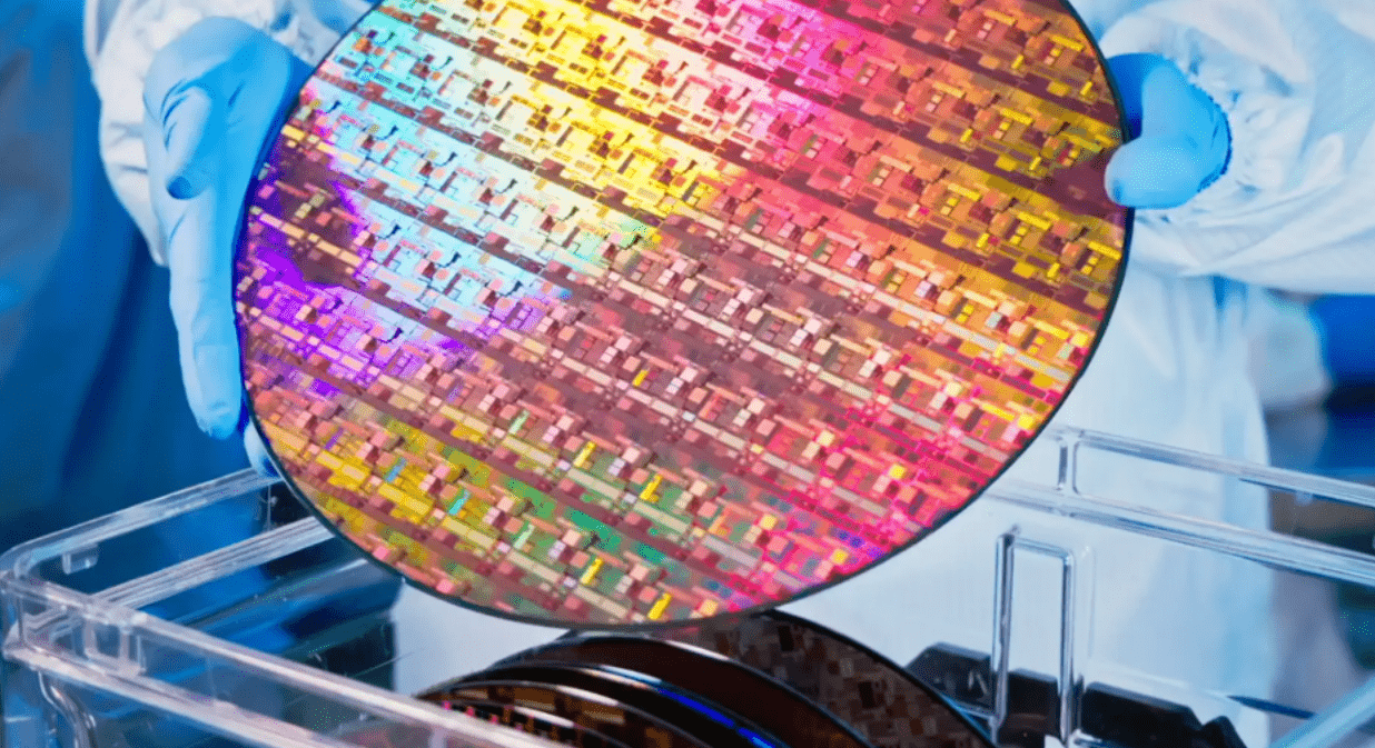
Nowadays, we use self-assembled monolayers in a number of sensors, energy devices, inks, and electronics. This is already a maturing technology that is impacting our lives, showing that nanoscale inventions can have a macroscopic impact on our lives.


