Extremely thin, semi-transparent and flexible solar cells are one step closer to becoming a reality. Scientists have managed to create a semiconductor structure consisting of two ultra-thin layers which is excellent for solar panels. The solar cells are also transparent, so they could be used as windows or glass fronts.
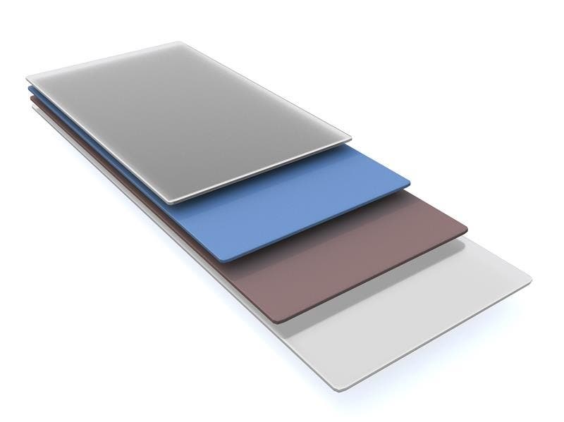
Several months ago, the team created the first layer, an ultra-thin layer of the photoactive crystal tungsten diselenide. Now, they have successfully combined it with another layer made of molybdenum disulphide, creating a system that could be used in the future generation of solar cells.
Ultra-thin materials, having only several atoms in thickness are a hot topic in science. The most notable example is graphene, the wonder material consisting of only 1 atom of thickness arranged in a lattice. We’ve already written how graphene could make the internet 100 times faster, how it can make incredibly resistant yarn which could revolutionize the textile industry, how it can give us predator vision, develop new transistors, repair itself naturally, and many more. But the good thing about graphene studies is that they didn’t just show us what graphene can do – it also showed us what other extremely thin materials can do. At the Vienna University of Technology, Thomas Mueller, Marco Furchi and Andreas Pospischil have put that knowledge to good use:
“Quite often, two-dimensional crystals have electronic properties that are completely different from those of thicker layers of the same material,” says Thomas Mueller. His team was the first to combine two different ultra-thin semiconductor layers and study their optoelectronic properties.
Tungsten diselenide was known to be able to transform solar energy into electricity and vice versa. It had a significant problem though – a solar cell made from it would require a huge number of tiny electrodes to properly function. For this reason, it was discarded from studies for a while. However, researchers found an elegant way around that using another layer of molybdenium disulphide, which also consists of three atomic layers. The exact mechanism through which it does this is rather complicated.
When light shines upon an object, photons displace electrons from their original position. Without the electron, which is negatively charged, a positively charged hole remains in place. Both the electron and the hole can move freely in the material, but here’s the thing – they only contribute with energy when they are kept apart, so they cannot recombine. In order to prevent recombination of electrons and holes, metallic electrodes can be used to suck the charge away.
The holes move inside the tungsten diselenide layer, the electrons, on the other hand, migrate into the molybednium disulphide,” says Thomas Mueller. Thus, recombination is suppressed.
Of course, this only works if the energy is tuned just right in both layers – but this can be ensured through electrostatic fields. Florian Libisch and Professor Joachim Burgdörfer (TU Vienna) used computer models to predict what energies changes are in both layers and what voltage leads to optimum energy yields.
“One of the greatest challenges was to stack the two materials, creating an atomically flat structure,” says Thomas Mueller. “If there are any molecules between the two layers, so that there is no direct contact, the solar cell will not work.”
Another advantage of this technology is that while part of the light is absorbed and creates energy, most of it passes right through, so these solar cells could be used as glass fronts.
Scientific Reference:
- Marco M. Furchi, Andreas Pospischil, Florian Libisch, Joachim Burgdörfer, Thomas Mueller. Photovoltaic Effect in an Electrically Tunable van der Waals Heterojunction. Nano Letters, 2014; 140728125936002 DOI: 10.1021/nl501962c
Was this helpful?


