homehome Home chatchat Notifications


Growing graphene nanoribbons jut got a lot easier, spelling great news for electronics

University of Wisconsin-Madison engineers devised a new method that grows graphene nanoribbons directly on a germanium wafer. The ribbons are of excellent quality and the technique is compatible with current manufacturing methods. These sort of ribbons have been heralded by industry experts as the component of the future which will make electronics faster and more efficient. The only thing that's been missing until now was a sound way to make them.

Tibi Puiu
August 12, 2015 @ 2:50 pm

share Share

University of Wisconsin-Madison engineers devised a new method that grows graphene nanoribbons directly on a germanium wafer. The ribbons are of excellent quality and the technique is compatible with current manufacturing methods. These sort of ribbons have been heralded by industry experts as the component of the future which will make electronics faster and more efficient. The only thing that’s been missing until now was a sound way to make them.
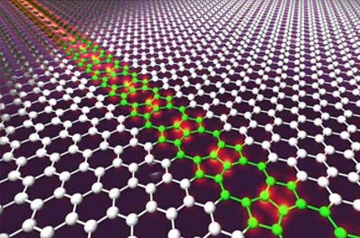
graphene

Image: extremetech

Graphene – the one atom thick carbon allotrope spaced in a hexagonal lattice – is a wonder material with fantastic electrical conductivity and heat dissipation. These properties makes it an ideal component in electronics, but graphene on its own is rather useless for semiconductor applications. For graphene to work as a semiconductor, it needs to be able to switch currents on and off. In more technical terms, previously scientists calculated that an optimal design would be a 10nm wide graphene with a well-defined edge where carbon-carbon bonds are parallel to the edge (the ‘armchair’ edge).

These sort of requirements are by no means easy to deliver. So far, two distinct approaches have been used to make the ribbons. One is “top-down” and involves cutting ribbons from a lithographically layered sheet of graphene. However, this method leads to ribbons with rough edges and variable size – a level of imprecision that is unpractical for use in high-grade electronics. The “bottom-up” method involves making the ribbons through chemical means from the ground up. Typically, various molecules react on a substrate surface where they polymerize into the ribbons. The quality of the ribbons is great, but the downside of the “bottom-up” method is that it only works on metal surfaces and the resulting ribbons are too short.
Zoom in of graphene nanoribbon on germanium. Image: Arnold Research Group

Zoom in of graphene nanoribbon on germanium. Image: Arnold Research Group

The UW-Madison researchers also used a “bottom-up” technique, with some key differences. Using chemical vapor deposition, the researchers carefully sprayed a germanium wafer with methane. Th methane gets adsorbed by the germanium wafer and eventually decomposes into graphene. Now, they key is to use methane in very small concentration to slow down the growth rate. At a low growth rate, the graphene crystals naturally grow into the ribbons.
“What we’ve discovered is that when graphene grows on germanium, it naturally forms nanoribbons with these very smooth, armchair edges,” said research leader Michael Arnold. “The widths can be very, very narrow and the lengths of the ribbons can be very long, so all the desirable features we want in graphene nanoribbons are happening automatically with this technique.”
“Graphene nanoribbons that can be grown directly on the surface of a semiconductor like germanium are more compatible with planar processing that’s used in the semiconductor industry, and so there would be less of a barrier to integrating these really excellent materials into electronics in the future,” Arnold said in a statement.
Besides fast electronics, the graphene nanoribbons can also be used to fashion chemical sensors which are very tiny and sensitive (very useful for detecting drugs or explosives). For the moment, Arnold and colleagues are concentrating on refining their method. For instance, they’ve yet to find a way to control the growth of the ribbons, i.e. choose where the ribbons start growing and in what direction.
Findings appeared in Nature Communications

share Share

A 2,300-Year-Old Helmet from the Punic Wars Pulled From the Sea Tells the Story of the Battle That Made Rome an Empire

An underwater discovery sheds light on the bloody end of the First Punic War.

Scientists Hacked the Glue Gun Design to Print Bone Scaffolds Directly into Broken Legs (And It Works)

Researchers designed a printer to extrude special bone grafts directly into fractures during surgery.

How Much Does a Single Cell Weigh? The Brilliant Physics Trick of Weighing Something Less Than a Trillionth of a Gram

Scientists have found ingenious ways to weigh the tiniest building blocks of life

A Long Skinny Rectangular Telescope Could Succeed Where the James Webb Fails and Uncover Habitable Worlds Nearby

A long, narrow mirror could help astronomers detect life on nearby exoplanets

Scientists Found That Bending Ice Makes Electricity and It May Explain Lightning

Ice isn't as passive as it looks.

The Crystal Behind Next Gen Solar Panels May Transform Cancer and Heart Disease Scans

Tiny pixels can save millions of lives and make nuclear medicine scans affordable for both hospitals and patients.

Satellite data shows New York City is still sinking -- and so are many big US cities

No, it’s not because of the recent flooding.

How Bees Use the Sun for Navigation Even on Cloudy Days

Bees see differently than humans, for them the sky is more than just blue.

Scientists Quietly Developed a 6G Chip Capable of 100 Gbps Speeds

A single photonic chip for all future wireless communication.

This Teen Scientist Turned a $0.50 Bar of Soap Into a Cancer-Fighting Breakthrough and Became ‘America’s Top Young Scientist’

Heman's inspiration for his invention came from his childhood in Ethiopia, where he witnessed the dangers of prolonged sun exposure.