MIT researchers develop printable electronics
MIT engineers have developed a fast, reliable and relatively cheap process through which they can print electronic surfaces.
MIT engineers have developed a fast, reliable and relatively cheap process through which they can print electronic surfaces. In a paper published today in Science Advances, the researchers report that they have fabricated carbon nanotube stamps able to print electronic ink onto both rigid and flexible surfaces.

MIT researchers have fabricated a stamp made from forests of carbon nanotubes that is able to print electronic inks onto rigid and flexible surfaces. Image credits: Sanha Kim and Dhanushkodi Mariappan
The key here is being able to print small enough transistors so that they can control individual pixels in high-resolution displays and touchscreens. This opens up a huge market for potential applications, although the full extent of this potential has not been gauged yet.
Sanha Kim, a postdoc in MIT’s departments of Mechanical Engineering and Chemical Engineering, is the lead author, and A. John Hart, the Mitsui Career Development Associate Professor in Contemporary Technology and Mechanical Engineering is the senior researcher.
“There is a huge need for printing of electronic devices that are extremely inexpensive but provide simple computations and interactive functions,” Hart says. “Our new printing process is an enabling technology for high-performance, fully printed electronics, including transistors, optically functional surfaces, and ubiquitous sensors.”
It’s not the first time something like this was attempted. Other teams have tried to print electronics using inkjet printing and rubber stamping techniques but results have generally been fuzzy – literally. Because the printing is very hard to control at small scales, the technique tends to produce “coffee-ring” botches, with the ink spilling outside the borders leading to incomplete or aberrant circuits.
“There are critical limitations to existing printing processes in the control they have over the feature size and thickness of the layer that’s printed,” Hart says. “For something like a transistor or thin film with particular electrical or optical properties, those characteristics are very important.”
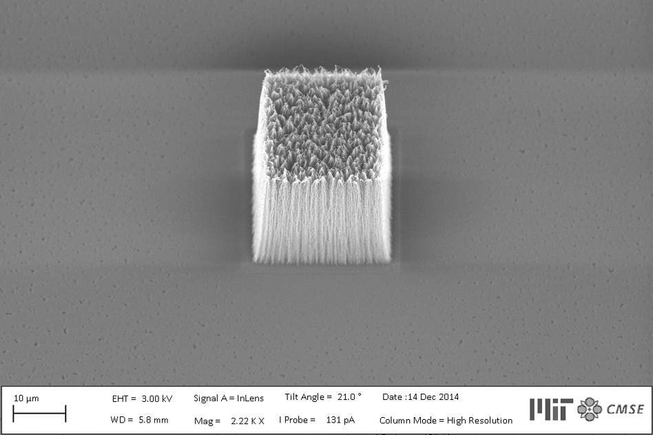
Professor A. John Hart and postdoc Sanha Kim hit upon the perfect material to create their highly detailed stamp: carbon nanotubes — strong, microscopic sheets of carbon atoms, arranged in cylinders. Image credits: Sanha Kim and Dhanushkodi Mariappan
This new technology uses “nanoporous” stamps to remedy that issue. Imagine a small, spongy stamp half the size of a normal fingernail, with pores thinner than the width of a human hair. These pores allow the “ink” to flow uniformly and ensure the printing precision and achieving very high resolution. The stamp itself is fabricated from carbon nanotubes – strong, microscopic sheets of carbon atoms, arranged in cylinders – arranged in forest-like patterns.
“It’s somewhat serendipitous that the solution to high-resolution printing of electronics leverages our background in making carbon nanotubes for many years,” Hart says. “The forests of carbon nanotubes can transfer ink onto a surface like massive numbers of tiny pen quills.”
The end result looked promising, and then they tested the electronics, to ensure that everything works fine. The patterns turned out to be indeed highly conductive and they worked as proper circuits.
Now, researchers are looking at three things: the first is how this process can be scaled up. They’ve already done the first steps, with a printing machine, including a motorized roller, and various substrates. Initial results show that this process could be scaled up and brought to industrial standards.
“This would be a continuous industrial process, where you would have a stamp, and a roller on which you’d have a substrate you want to print on, like a spool of plastic film or specialized paper for electronics,” Hart says. “We found, limited by the motor we used in the printing system, we could print at 200 millimeters per second, continuously, which is already competitive with the rates of industrial printing technologies. This, combined with a tenfold improvement in the printing resolution that we demonstrated, is encouraging.”
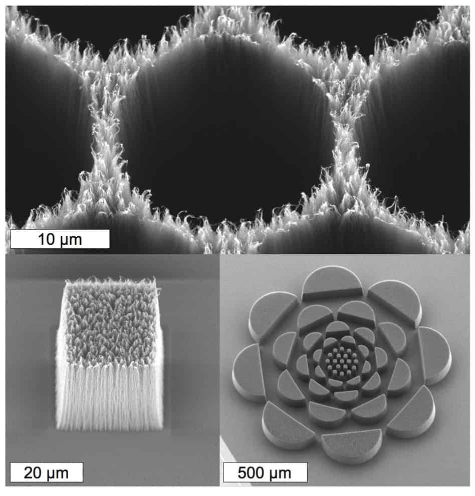
These scanning electron microscopy images show nanoporous stamps composed of pPFDA coated carbon nanotubes. Image credits: Sanha Kim and Dhanushkodi Mariappan
The second thing is finding applications for this technology. There might be a small emerging market for printable electronics, but just how large the demand is remains to be seen. Lastly, the team is already looking at ways to make this technology even more advanced – especially through graphene.
“Another exciting next step is the integration of our printing technologies with 2-D materials, such as graphene, which together could enable new, ultrathin electronic and energy conversion devices,” Hart says.
Journal Reference: Ultrathin high-resolution flexographic printing using nanoporous stamps.